The William H. Miller III Department of Physics and Astronomy houses research instrumentation that can utilized by appointment or through association. Below is a listing of potentially available instruments and who to contact for more information about each instrument.
The Instrument Development Group (IDG) is a service center specializing in the development of instrumentation for research in astronomy, condensed matter physics and the natural sciences.
Condensed Matter Physics Lab
Some of this equipment can be scheduled by registered and approved users. To request registration, please email [email protected]. Scheduling occurs via Google calendar. You can inspect the current schedule for each scheduled piece of equipment. Once registered users can reserve time on scheduled equipment by accessing the corresponding calendar through their google calendar account. To schedule this equipment, please use the calendar.
View the instructions on how to access the equipment remotely.
Optical Floating Zone Furnaces
Halogen optical floating zone furnace – Crystal growth using a four mirror image furnace has been used to grow and study a variety of bulk crystals, particularly single crystals of metal oxides.
In the optical floating zone technique, the basic concept is that four ellipsoidal mirrors are used to focus the light from halogen (or xenon) lamps onto a vertically held rod shaped sample to produce a molten zone, which is then moved along the sample in order to grow a single crystal. The maximum operating temperature of halogen and xenon furnaces are ~2200 C and ~3000 C respectively; and gas pressures of up to 10 bar (1.0 MPa) can be used within the growth chamber.
Xenon optical floating zone furnace – The use of light heating makes the technique suitable for both conducting and non-conducting materials, a feature that distinguishes image furnace growth from float zoning using induction or electron beam heating, both of which are limited to use with conductors. Although light heating is not suited to all materials (it struggles, for example, with those metallic samples that exhibit a high reflectivity in the infra red region), it is particularly convenient and efficient for those oxides and semiconductors that absorb infrared easily. Thus, probably the group of materials for which image furnace growth has been most used are what may be termed functional oxides, crystals of which find applications in lasers, electronic and optical devices, catalysts, solid oxide fuel cells, memory and magnetic devices, oxygen and magneto-optical sensors and as superconducting materials.
Other Furnaces
Horizontal and vertical tube furnaces and Box furnaces – Furnaces including box furnaces (max. temp. 1200C and 1700C), horizontal tube furnace (max. 1200C) and vertical tube furnace (max. 1800C) are operated to perform solid state reactions and sintering procedures for preparing powders, and feed rods that can be used in the image furnace.
Physical Property Measurement System
Physical Property Measurement System (PPMS) – The Physical Property Measurement System is a versatile instrument that measures a broad range of magnetic, transport, electro-transport and thermal transport properties of systems. Heat capacity, AC and DC resistivities, thermal conductivity, ac susceptibility, DC magnetization and the Hall Effect are just some examples of properties of bulk or thin lm samples that can be measured using this system. In addition, our Quantum Design PPMS is supplemented by a state-of-the-art Dilution Refrigerator that operates at a wide range of temperatures from room temperature down to 50 mK. To schedule use of the PPMS, use the above calendar.
X-Ray Laue Equipment
X-ray laue equipment – Grown crystals are aligned using the back-reflection X-ray technique. In this technique, the conditions for diffraction are met by using “white” X-rays, i.e., a continuous spectrum. Thus, although the specimen is a fixed single crystal, the variable necessary to ensure that Bragg’s law is satisfied for different sets of planes in the crystal, is provided by the range of wavelengths in the beam. Thus each set of crystal planes chooses the appropriate value lambda, from the “white” spectrum to give a reflection according to Bragg’s law, n(lambda)=2dsin(theta).
Bulk Crystal Growth Facility
The PARADIM bulk crystal facility is located at Johns Hopkins University. Together with the thin film growth facilities at Cornell, it provides unprecedented capabilities for discovery of new materials and interfaces.
The PARADIM Bulk Crystal Facility is the only facility within the United States where all major optical FZ techniques are available at a single site. In addition, it is the first location in the world to have optical floating zone capability at 300 atm.
Advanced capabilities include:
- Halogen Four Mirror Optical Floating Zone Furnace
- Xenon Four Mirror Optical Floating Zone Furnace
- A tilting laser diode optical floating zone furnace (Tilt-LDFZ) – the first in the world to combine laser diode heating with real-time control of laser source tilting
- The world’s first high pressure optical floating zone (HPFZ) furnace capable of operations at up to 300 atm in inert and reactive gas atmospheres
- An Ultrahigh Temperature Vacuum Furnace with Bridgeman/CZ pullers
- A vertical furnace with Bridgeman/CZ pullers
- Real-time Laue for Sample Alignment and Cutting
- A high temperature induction furnace – capable of Bridgeman/FZ growth at MBE wafer scale (1/2”-1” diameter),
- Spark Plasma Sintering Furnace,
- Two high resolution, high dynamic range mass spectrometers for in situ chemical characterization during growth,
- An inert-environment glovebox, and
- Associated sample preparation and characterization facilities
Some of these facilities are available via a cooperative agreement with the Institute for Quantum Matter; others are new and provided by the PARADIM cooperative agreement. In either case, however, they are available to PARADIM users through the PARADIM user program.
View the Crystal Growth Facility User Facility Guide. Questions regarding PARADIM bulk crystal facilities and capabilities should be addressed to Prof. McQueen or Dr. Phelan.
Fabrication and Processing
Cleanroom
The cleanroom within Bloomberg Center is a class 1000 environment with temperature and humidity control and features contact and projection photolithography equipment, a thermal evaporator and video microscopy capabilities. Contact: Dan Reich
As of July 1, 2017, the rate to use the clean room is $15 per hour.
Photolithography
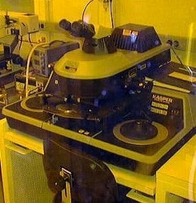
Mask Aligner
- Contact photolithography across 3” wafer with 2 micron feature size
- Multiple-mask alignment with 2 micron accuracy
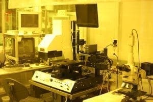
Projection Photolithography
- 0.5 micron feature size
Thermal Evaporator
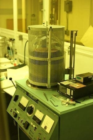
- Multiple-Source Supttering Chambers – 4, 6 source systems with 2-inch targets, DC and RF magnetron sputtering and a computer-controlled multilayer deposition system. A ten-source sputtering chamber is also available. Contact: Chia-Ling Chien
- Pulsed Laser – Lambda-Physik Pulsed Laser Deposition System Contact: Chia-Ling Chien
- Tubular Furnaces – Up to 1500o C. Contact: Chia-Ling Chien
- Wire Bonder – Kulicke & Soffa 4523 Wire Bonder. Features: 30 and 45 degree wedge bonder; 25, 75 micron wire; 50 micron pad size. Contact: Chia-Ling Chien
- FEI Nova 600 Dual-Beam Focused Ion Beam System – Contact: Chia-Ling Chien
Measurement of Physical Properties
Raman Spectrometer
Raman scattering is an important tool for materials characterization and fundamental research in condensed matter physics. The T64000 Jobin-Ivon Horiba triple monochtomator spectrometer CCD LN2 cooled detector in our laboratory allows both. Contact: Natalia Drichko
Raman scattering is an important tool for materials characterization and fundamental research in condensed matter physics. The equipment in our Raman laboratory allows both.
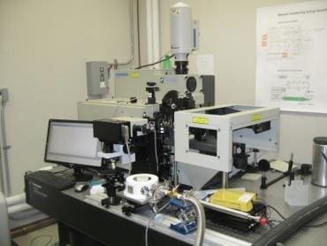
The basic setup of the Raman Lab within the William H. Miller III Department of Physics & Astronomy is as follows:
T64000 Jobin-Ivon Horiba triple monochtomator spectrometer CCD LN2 cooled detector
- Raman shifts down to 5 cm-1
- Spectral resolution down to 2 cm-1
- Single monochromator option (514.5 nm, down to 50 cm-1) for measurements of very low signals
Ar+Kr ion Spectra-Physics laser: excitation lines in the range from 488 to 672 nm makes resonance Raman measurements possible.
Micro-Raman measurements: using an Olympus microscope allows us to measure small samples of various configurations, this method is extremely useful for material science and characterization of crystals of new material
- Sampling probe diameter 2 μm
- Frequency range: down to 50 cm-1
- Measurements at temperatures 300-4 K
We are also equipped with the possibilities of mapping of the sample surface using Raman scattering:
- An automatic mapping stage allows mapping of a sample surface 1 cm*1 cm with spatial resolution 2mm
- Duoscan option allows mapping of a surface 20mm* 20mm with spatial resolution 0.5 mm.
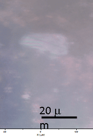
An example of micro-Raman measurement at low temperatures:
Measured at 20 K single crystal of KNi2Se2 sealed in a quartz capillary
- Helium Liquefier – Condensed matter physicists and astronomers in the department use liquefied helium to create extremely cold research conditions (often just a few degrees above absolute zero). The helium liquefier within Bloomberg Center creates a stable and affordable supply of liquid helium for the department. It can store 500 liters of liquid helium. Contact: Peter Armitage
- Quantum Design SQUID Magnetometer – Features: 5 Tesla superconducting magnet; 1.7K to 400K; 1uemu sensitivity. Contact: Chia-Ling Chien
- Vector Vibrating Sample Magnetometer – ADE Technologies Model 10 Vector Vibrating Sample Magnetometer. Features: 3 Tesla maximum field; 0.01 Oe field resolution; micro-emu sensitivity; 1.5 degree angular resolution; 100 K – 700 K sample temperature; simultaneous measurement of two components of magnetization. Contact: Chia-Ling Chien
- Rheometer – Anton-Paar model MCR300. Contact: Robert Leheny
- Magneto-Transport Measurement System – Contact: Chia-Ling Chien
- Andreev Reflection Spectroscopy – Contact: Chia-Ling Chien
X-Ray Characterization
Philips 3720 X-Ray Diffraction System – Contact: Chia-Ling Chien
Philips X’Pert MRD Diffractometer – Features: Three detectors, angular resolution up to 0.003 degrees; Pole figures; Low angle relectometry; Seven-axis sample positioning. Contact: Chia-Ling Chien
Electron Microscopy
Zeiss SEM and Electron Beam Lithography System – Contact: Chia-Ling Chien
Surface Characterization
Tencor Thin Film Profilometer – Contact: Chia-Ling Chien
AFM/MFM – Contact: Chia-Ling Chien
